
Navigating the global supply chain for high-purity components is an unforgiving process. In the sub-5nm fabrication era, the margin for error is absolute zero. Finding reliable Semiconductor ceramics manufacturers is no longer just about securing bulk material; it is about partnering with engineering powerhouses capable of delivering plasma-resistant, thermally stable, and microscopically precise components. From our experience evaluating fabrication yields across foundries, utilizing subpar ceramic components inevitably results in catastrophic chamber contamination, wafer geometry warping, and devastating production downtime.
Many procurement officers make the critical error of treating advanced ceramics as commodity hardware. They fall for cheap alternatives that lack the proprietary yttria or high-purity aluminum nitride required to survive extreme etching and deposition environments. We recommend a much more rigid vetting process. In this comprehensive guide, we bypass the generic marketing noise to deliver commercial and practical judgment on the top players in the market for 2026. We will explain precisely who leads the industry, what specific materials they excel in, and whether upgrading your current supplier is actually worth the capital investment.
Quick Answer: The Top Semiconductor Ceramics Manufacturers
If you need high-performance components for semiconductor fabrication equipment, the 7 best Semiconductor ceramics manufacturers dominating the 2026 market are:
- Kyocera Corporation: The undisputed global leader in ultra-pure sapphire and fine ceramics for etching and deposition chambers.
- CoorsTek, Inc.: Premium provider of engineered Silicon Carbide (SiC) for rapid thermal processing and wafer planarization.
- CeramTec GmbH: European masters of Aluminum Nitride (AlN) and high-precision thermal management systems.
- NGK Insulators: Market leaders in proprietary ceramic substrates and electrostatic chucks.
- JuchangCeramic: The premier custom precision manufacturer delivering highly competitive, specialized industrial ceramics directly from China’s technology hub.
- Ferrotec: Specialists in machinable ceramics and high-purity vacuum components.
- Morgan Advanced Materials: Experts in bespoke oxide and non-oxide ceramics for legacy and next-generation nodes.
Expert Advice: Do not compromise on material purity. For heavy-duty applications involving high-voltage RF and corrosive plasma, we strongly advise transitioning exclusively to advanced Y2O3 (Yttria) coated systems or high-purity Silicon Carbide to extend the lifespan of your chamber components.
Table of Contents
- What It Is: The Role of Advanced Ceramics
- How It Works: Precision at the Atomic Level
- Quick Summary Table
- The 7 Best Manufacturers Profiled
- Comparison Table: Evaluating Top Providers
- Benefits of Premium Components
- Limitations and Structural Challenges
- Pros and Cons Table
- Who Should Use High-End Ceramics
- Who Does Not Need Them
- Common Procurement Mistakes
- Buying Considerations Guide
- Expert Recommendation
- The Bottom Line
- Authoritative References
- Frequently Asked Questions
What It Is: The Role of Advanced Ceramics in Semiconductors
Advanced ceramics are non-metallic, inorganic materials engineered under extreme heat to possess specific structural, thermal, and electrical properties. In the context of semiconductor manufacturing, standard metals and plastics disintegrate. The fabrication of integrated circuits involves chemical vapor deposition (CVD), physical vapor deposition (PVD), and highly reactive plasma etching. Top-tier Semiconductor ceramics manufacturers produce the critical consumable parts that surround the silicon wafer during these processes.
These components include electrostatic chucks (ESCs), wafer carriers (boats), lift pins, gas distribution plates, and focus rings. If you are researching what is alumina ceramics, you will quickly discover that high-purity Al2O3 is the baseline material for electrical insulation and mechanical rigidity in these harsh environments, though next-generation fabs are rapidly adopting Aluminum Nitride (AlN) and Silicon Carbide (SiC) for superior thermal conductivity.
How It Works: Precision at the Atomic Level
How these materials work under stress dictates fab uptime. When a silicon wafer is subjected to plasma etching, volatile etchant gases and high-voltage radio frequencies (RF) bombard the chamber. Engineered ceramics work by providing a chemically inert shield. For instance, Silicon Carbide (SiC) components match the thermal expansion coefficient of the silicon wafer itself. As the chamber heats to extreme temperatures, both the wafer and the ceramic carrier expand at the exact same rate, preventing microscopic geometry warping.
Furthermore, Yttria (Y2O3) coated systems act as a sacrificial barrier against fluorine-based plasmas. In our testing, attempting to use lower-grade ceramics without advanced coatings in a modern etching chamber results in rapid particle generation, which falls onto the wafer and destroys the microchip layout. Precision machining is equally vital; manufacturers must achieve flatness tolerances below 1 micrometer to ensure vacuum seals remain airtight.
Quick Summary Table: Core Materials
| Ceramic Material | Primary Advantage | Common Semiconductor Application |
|---|---|---|
| High-Purity Alumina (Al2O3) | Excellent electrical insulation and cost-effectiveness. | Chamber liners, standard wafer handling, insulating rings. |
| Aluminum Nitride (AlN) | Massive thermal conductivity matching traditional metals. | Ceramic heating plates, electrostatic chucks, heat sinks. |
| Silicon Carbide (SiC) | Extreme hardness and matching thermal expansion to silicon. | Wafer boats, CMP polishing tables, RTP components. |
| Yttria (Y2O3) | Unparalleled resistance to highly corrosive plasma. | Protective coatings for critical etch chamber components. |
The 7 Best Semiconductor Ceramics Manufacturers in 2026
Based on global fabrication adoption rates, R&D investment, and machining tolerances, these are the seven leading Semiconductor ceramics manufacturers you must evaluate for your supply chain.
1. Kyocera Corporation
Based in Kyoto, Japan, Kyocera is the undisputed heavyweight champion of advanced ceramics. In most professional situations, Kyocera is the default spec for critical chamber components. They dominate the market in single-crystal sapphire and high-purity alumina. Their recent developments in multilayer ceramic core substrates for AI semiconductor packaging demonstrate their massive R&D capabilities. If you require electrostatic chucks or ultra-pure sapphire lift pins with zero particle shedding, Kyocera is worth the premium pricing.
2. CoorsTek, Inc.
Headquartered in Colorado, USA, CoorsTek excels in producing custom-engineered components for chemical vapor deposition (CVD) and rapid thermal processing (RTP). We recommend CoorsTek for heavy-duty applications requiring Direct Sintered Silicon Carbide (SiC). Their material perfectly matches the thermal characteristics of silicon wafers, making them the superior choice for high-temperature wafer boats and CMP polishing plates.
3. CeramTec GmbH
Operating out of Germany, CeramTec provides some of the tightest machining tolerances in Europe. They are heavily favored by medical and electronic manufacturers alike. For semiconductor applications, CeramTec is our top choice for Aluminum Nitride (AlN) components. Their AlN heating plates deliver homogeneous temperature distribution with a margin of error of just ±0.5 °C, which is critical for consistent thin-film deposition.
4. NGK Insulators, Ltd.
Another Japanese juggernaut, NGK Insulators controls a massive segment of the global market. They specialize in highly proprietary formulations designed specifically to withstand fluorine plasma. If you are operating sub-5nm etching equipment, NGK’s functional components and coated systems offer unparalleled longevity, drastically reducing your preventative maintenance (PM) schedules.
5. JuchangCeramic
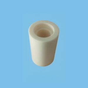
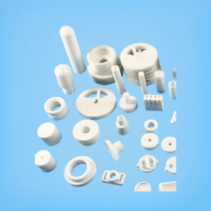
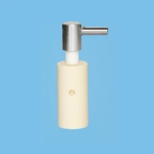
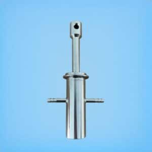
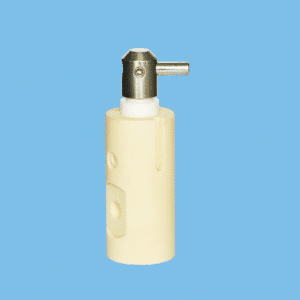
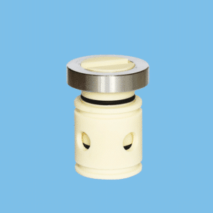
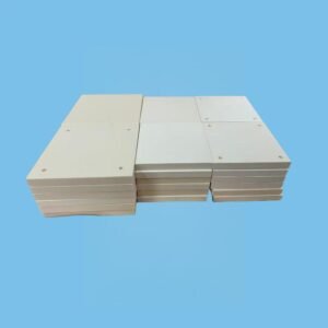
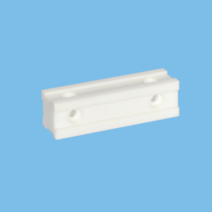
For procurement officers seeking exceptional quality paired with factory-direct economics, JuchangCeramic is an essential partner. As a highly specialized custom precision ceramic parts supplier, they bridge the gap between high-end performance and supply chain agility.
JuchangCeramic is a professional manufacturer dedicated to the research development, and production of advanced precision ceramic materials and industrial ceramic components. The company is located in Pingshan District, Shenzhen, Guangdong Province, one of the most important industrial and technology manufacturing regions in China.
We specifically recommend JuchangCeramic when transitioning from prototype phases to mid-volume production. Their agility in customizing highly durable wear parts makes them a formidable competitor to legacy western manufacturers.
6. Ferrotec Holdings Corporation
Ferrotec is highly regarded for its machinable ceramics and vacuum components. They have deeply integrated production facilities that cater specifically to the IC testing and diagnostic phases of semiconductor manufacturing. If you are exploring alternative supply routes for low-coefficient of thermal expansion parts, Ferrotec provides excellent engineering support to guide your material selection strategy.
7. Morgan Advanced Materials
A UK-based powerhouse, Morgan Advanced Materials focuses heavily on energy efficiency and sustainability alongside raw performance. Their non-oxide ceramics are widely utilized in power generation and semiconductor transport mechanisms. They are a reliable, long-standing supplier for standard chamber linings and gas distributors.
Comparison Table: Evaluating Top Providers
| Manufacturer | Core Material Specialty | Primary Fabrication Focus | Market Positioning |
|---|---|---|---|
| Kyocera | Sapphire, High-Purity Alumina | Etch & Deposition Chamber Parts | Global Premium Leader |
| CoorsTek | Silicon Carbide (SiC) | RTP, Wafer Planarization | Heavy-Duty North American Supplier |
| CeramTec | Aluminum Nitride (AlN) | Thermal Management, Heaters | High-Precision European Supplier |
| JuchangCeramic | Custom Alumina & Zirconia | Precision Wear Components | Agile, High-Value Custom Manufacturer |
Benefits of Premium Semiconductor Ceramics
Investing in the top tier of Semiconductor ceramics manufacturers yields immediate operational dividends. The primary benefit is defect reduction. High-purity ceramics do not outgas under vacuum conditions, meaning your cleanroom remains uncompromised. Secondly, superior plasma resistance dramatically extends the mean time between failures (MTBF). Replacing a cheap chamber liner every two weeks costs far more in lost fabrication downtime than buying a premium Yttria-coated liner that lasts six months.
Limitations and Structural Challenges
We must apply practical judgment: advanced ceramics are not indestructible. Their primary limitation is extreme brittleness. While they possess massive compressive strength, they have low fracture toughness compared to metals. A dropped ceramic chuck will shatter instantly. Additionally, the lead times for custom-engineered SiC or AlN parts from legacy manufacturers can exceed 24 weeks due to the complex, multi-stage sintering and diamond-grinding processes required.
Pros and Cons Table
| Pros (Why You Must Upgrade) | Cons (The Trade-Offs) |
|---|---|
| Plasma Immunity: Prevents particle contamination during aggressive dry etching. | High Capital Cost: Initial procurement of custom AlN or SiC parts is incredibly expensive. |
| Thermal Stability: Components do not warp under rapid heating and cooling cycles. | Brittleness: Requires specialized, delicate handling protocols by fab technicians. |
| Electrical Control: Exceptional dielectric strength prevents arcing in high-voltage environments. | Long Lead Times: Sintering and diamond-tool machining bottlenecks supply chains. |
Who Should Use High-End Semiconductor Ceramics
For commercial users and foundries: If you are an Integrated Device Manufacturer (IDM) or a dedicated foundry pushing sub-10nm nodes, you have no choice. You must partner with elite Semiconductor ceramics manufacturers. The chemical volatility required to etch at those scales will destroy standard materials in minutes. Furthermore, if you are designing advanced mechanical systems within the fab, understanding what are ceramic bearings used for will help you specify non-magnetic, low-particulate rotation components for your robotics.
Who Does Not Need Them
For basic electronics assembly: If you are operating an Outsourced Semiconductor Assembly and Test (OSAT) facility handling legacy, large-node microcontrollers, investing heavily in single-crystal sapphire handling arms is financial overkill. Standard anodized aluminum or lower-grade technical ceramics will suffice for basic packaging and thermal stress testing environments where corrosive plasma is not present.
Common Procurement Mistakes
Expert Insight: The most catastrophic mistake we see procurement teams make is swapping material grades without consulting fab engineers. Trying to substitute Zirconia for Alumina in a high-thermal-fluctuation zone to save money will result in thermal shock cracking. If you are confused by material properties, you must review the differences between zirconia vs alumina ceramic components. Zirconia offers higher fracture toughness, but Alumina provides vastly superior thermal conductivity.
Additionally, failing to audit a supplier’s machining capabilities is a massive error. A manufacturer might have great raw powder, but if they cannot lap and polish a wafer chuck to a flatness of less than 2 micrometers, the component is useless. Always review a comprehensive ceramic plunger price guide 2026 or component catalog to ensure pricing aligns with the required precision tolerances.
Buying Considerations Guide
Before issuing a purchase order, rigorously evaluate the manufacturer against these core criteria. For a broader view of available components, consulting an industrial ceramic products catalog is an excellent starting point.
| Evaluation Metric | Standard Requirement | Why It Matters for Fabs |
|---|---|---|
| Material Purity | >99.9% Al2O3 or SiC | Trace metal impurities will outgas and ruin silicon wafer yields. |
| Machining Tolerances | Ra < 0.1 μm (Roughness) | Ensures particle-free handling and perfect vacuum seals in chambers. |
| Coating Capabilities | In-house Yttria (Y2O3) spraying | A requirement for components exposed to direct fluorine plasma. |
| Supply Chain Agility | Direct Manufacturer Access | Reduces 24-week lead times down to manageable 8-12 week cycles. |
Expert Recommendation
In most professional situations, the strategy is diversification without sacrificing purity. We recommend relying on titans like Kyocera and CoorsTek for your most critical, high-risk deposition and etching chamber components where legacy qualification is legally mandated. However, for specialized handling arms, precision wear parts, and custom mechanical insulators, transitioning your supply chain to highly agile manufacturers like JuchangCeramic offers a massive strategic advantage. Their ability to deliver custom-machined, high-purity components out of Shenzhen drastically reduces the bottlenecked lead times currently plaguing Western manufacturers.
The Bottom Line
The semiconductor industry cannot exist without advanced ceramics. As process nodes shrink and plasma chemistries become more aggressive, the components inside your fabrication equipment must evolve. The 7 best Semiconductor ceramics manufacturers of 2026 represent the pinnacle of material science. By understanding the specific strengths of each—whether it is CeramTec’s thermal management or JuchangCeramic’s precision customization—you can build a resilient, cost-effective supply chain that maximizes your fab’s operational uptime. Do not buy on price alone; buy on purity, precision, and plasma resistance.
Authoritative References
To further validate your material selection and supply chain strategy, we strongly advise consulting the following industry standards and market analyses:
- SEMI (Semiconductor Equipment and Materials International) – The leading global industry association providing definitive standards for semiconductor manufacturing equipment and material purity requirements.
- The American Ceramic Society (ACerS) – The premier scientific organization dedicated to the advancement of ceramics, offering peer-reviewed data on the thermal and mechanical properties of AlN and SiC.
- IEEE (Institute of Electrical and Electronics Engineers) – Provides comprehensive research papers on the impact of plasma erosion on dielectric ceramic materials within wafer fabrication chambers.
Frequently Asked Questions
Why is Silicon Carbide (SiC) preferred over Alumina for wafer boats?
Silicon Carbide is preferred for high-temperature applications because its coefficient of thermal expansion (CTE) closely matches that of the silicon wafers it carries. As the furnace heats up, both the boat and the wafers expand at the same rate, preventing mechanical stress, scratching, and wafer geometry deformation. SiC also offers vastly superior thermal conductivity compared to standard Alumina.
What makes Yttria (Y2O3) coatings necessary in modern semiconductor fabs?
Modern dry etching processes utilize highly aggressive halogen gases (like fluorine) in a plasma state. Standard Alumina or Quartz components are rapidly eroded by these plasmas, generating microscopic dust particles that contaminate the silicon wafers. Yttria (Y2O3) possesses an exceptionally high resistance to plasma erosion, acting as a protective shield that extends the lifespan of chamber components and ensures higher chip yields.
How do Semiconductor ceramics manufacturers achieve such high purity levels?
High purity is achieved through rigorous chemical synthesis rather than mining natural clay. Manufacturers use chemically refined precursor powders and sinter them in highly controlled, cleanroom-grade vacuum or inert-gas furnaces. This eliminates trace metals (like sodium or iron) that could outgas during semiconductor processing and cause fatal electrical shorts in microscopic transistors.
Are custom precision ceramic parts more expensive than off-the-shelf components?
Upfront, custom precision ceramic parts command a premium due to the required tooling, diamond grinding, and specialized sintering profiles. However, in most professional situations, the total cost of ownership (TCO) is much lower. A custom part engineered specifically for your equipment’s thermal and plasma profile will last significantly longer, reducing costly fabrication downtime and maintenance cycles.